


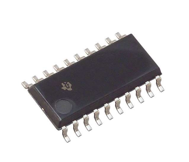
SN74HC541NSR
SN74HC541NSR characteristics • Wide operating voltage range from 2V to 6V • High current 3-state output can directly drive bus lines or up to 15 LSTTL loads • Low power consumption, maximum ICC of 80 μ A • Typical TPD=10ns • Output driving current of ± 6mA at 5V • Low input current (maximum value of 1 μ A) • Data flow pin arrangement (all inputs are located on the other side of the output)
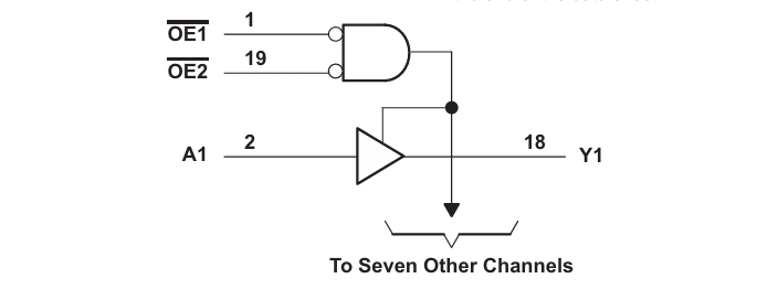
SN74HC541NSR These eight channel buffers and line drivers have the performance of SNx4HC541 devices, with pins arranged on opposite sides of the package for input and output. This arrangement greatly facilitates the layout of printed circuit boards. The three state output is controlled by a dual input NOR gate. If any output enables (OE1 or OE2) input to be high, then all 8 outputs are in a high impedance state. The SN74HC541NSR device provides real data at the output end.
SN74HC541NSR applied to • LED • servers • personal and laptop computers • wearable health and wellness devices • electronic sales points
Attachment Download
Previous article:
TLV70215DBVRNext article:
TLV71721PDQNRCopyright 2019-2024 All rights reserved by Shenzhen Lites Electronic Technology Co., Ltd Record number:Yue ICP Bei 18031876-1